Students can access the CBSE Sample Papers for Class 12 Physics with Solutions and marking scheme Set 2 will help students in understanding the difficulty level of the exam.
CBSE Sample Papers for Class 12 Physics Set 2 with Solutions
Time : 3 Hours
Maximum Marks: 70
General Instructions :
- There are 33 questions in all. All questions are compulsory.
- This question paper has five sections: Section A, Section B, Section C. Section D and Section E.
- Air the sections are compulsory.
- Section A contains sixteen questions, twelve MCQ and four Assertion-Reasoning based questions of 1 mark each, Section B contains five questions of two marks each, Section C contains seven questions of three marks each, Section D contains two case study-based questions of four marks each and Section E contains three long answer questions of five marks each.
- There is no overall choice. However, an internal choice has been provided in one question in Section B, one question in Section C, one question in each CBQ in Section D and all three questions in Section E. You have to attempt only one of the choices in such questions.
- Use of calculators is not allowed.
- You may use the following values of physical constants wherever necessary
(i) c = 3 ×10⁸ m/s
(ii) me = 9.1 × 10⁻³¹ kg
(iii) e = 1.6 × 10⁻¹⁹ C
(iv) μ0= 4π × 10-17 TmA-1
(v) h = 6.63 × 10⁻³⁴ Js
(vi) ε0 = 8.854 ×10⁻¹² C2N-1m-2
(vii) Avogadro’s number = 6.023 × 10²³ per gram mole
Section – A
The following questions are multiple-choice questions with one correct answer. Each question carries 1 mark. There is no internal choice in this section.
Question 1.
If charge q is placed at the centre of the line joining two equal charges Q, the system of these charges will be in equilibrium if q is:
(a) -4Q
(b) -Q/4
(c) -Q/2
(d) +Q/2
Answer:
(b) -Q/4
Explanation: For equilibrium, net force on Q = 0.
Let, the distance between line joining two equal charges Q is x unit.
∴ \(\frac{k \mathrm{QQ}}{(2 x)^2}+\frac{k q \mathrm{Q}}{x^2}=0\)
∴ q =-Q/4
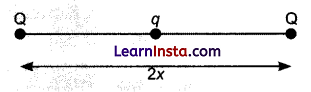
q =-Q/4
Question 2.
The electric potential inside a conducting sphere:
(a) increases from centre to surface
(b) decreases from centre to surface
(c) remains constant from centre to surface
(d) is zero at every point inside
Answer:
(c) remains constant from centre to surface
Explanation: Electric potential inside a conductor is constant and it is equal to that on the surface of the conductor.
![]()
Question 3.
According to the Kirchhoffs law, in any analytic circuit, if the direction of current assumed to be opposite, then the value of current will be:
(a) i
(b) 2i
(c) – i
(d) 0
Answer:
(c) -i
Explanation: According the Kirchhoff’s law, in any analytic circuit, if the direction of current assumed to be opposite, then the value of current will be – i.
Question 4.
A particle of mass m and charge q enters a magnetic field B perpendicularly with a velocity v. The radius of the circular path described by it will be:
(a) \(\frac{m q}{\mathrm{~B} v}\)
(b) \(\frac{\mathrm{B} q}{m v}\)
(c) \(\frac{m v}{\mathrm{~B} q}\)
(d) \(\frac{m \mathrm{~B}}{q v}\)
Answer:
(c) \(\frac{m v}{\mathrm{~B} q}\)
Explanation:
Force, F = qvB =\(\frac{m v^2}{\mathrm{R}}\)
\(\mathrm{R}=\frac{m v}{\mathrm{~B} q}\)Question 5.
A 2 MeV proton is moving perpendicular to a uniform magnetic field of 2.5 T. The force on the proton is:
(a) 2.5 × 10⁻¹⁰ N
(b) 2.5 × 10⁻¹¹ N
(c) 7.6 × 10⁻¹¹ N
(d) 7.85 × 10⁻¹² N
Answer:
(d) 7.85 × 10⁻¹² N
Explanation: We know that,
F = qvB
\(=1.6 \times 10^{-19} \times\left(\sqrt{\frac{2 \mathrm{E}}{m}}\right) 2.5\)
= 7.85 × 10⁻¹² N
Question 6.
The magnetic dipole moment of a solenoid having N turns is given as:
(a) NIA
(b) NLA²
(c) NI²A
(d) NI²A²
Answer:
(a) NIA
Explanation: Each turn of the solenoid behaves as a small dipole having dipole moment IA. Hence, the magnetic dipole moment of a solenoid having N turns = NIA
![]()
Question 7.
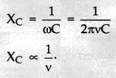
Which of the following curves correctly represent the variation of capacitive reactance (Xc) with frequency (v)?
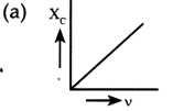
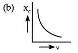
Answer:

Explanation: We know that,
Question 8.
Which of the following can act as a source of electromagnetic waves?
(a) A charge at rest
(b) A charge moving with a constant velocity
(c) A charge moving in a circular orbit
(d) None of these
Answer:
(c) A charge moving in a circular orbit
Explanation: A charge moving in a circular orbit can act as a source of electromagnetic waves as the e.m. waves are produced by accelerated charged particles only. A charge moving in a circular orbit has an accelerated motion.
![]()
Question 9.
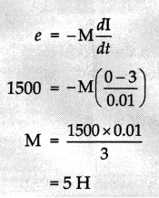
If a current of 3 A flowing in the primary coil is reduced to zero in 0.01 s then the induced emf in the secondary coil is 1500 V, the mutual inductance between the two coils is:
(a) 0.5 H
(b) 1.5 H
(c) 5 H
(d) 10 H
Answer:
(c) 5 H
Explanation:
Question 10.
Young’s double slit arrangement is contained in a transparent chamber. If the chamber is evacuated, then :
(a) fringes will disappear
(b) fringe width will slightly increase
(c) fringe width will slightly decrease
(d) there will be no effect
Answer:
(d) there will be no effect
Explanation: Young’s double slit arrangement is contained in a transparent chamber. If the chamber is evacuated, then the position of maxima and minima will change but there will be no effect on fringe width.
Question 11.
Work function of a photoelectric material is 3.3 eV. What will be its threshold frequency?
(a) 8 × 10¹⁰ Hz
(b) 8 × 10¹⁴ Hz
(c) 8 × 10²⁰ Hz
(d) 8 × 1025 Hz
Answer:
(b) 8 × 10¹⁴ Hz
Explanation:
\(f=\frac{3.3 \times 1.6 \times 10^{-19} \mathrm{~J}}{6.626 \times 10^{-34} \mathrm{~J}-\mathrm{s}}=8 \times 10^{14} \mathrm{~Hz}\)
![]()
Question 12.
If Ep and Ek represent potential energy and kinetic energy respectively, of an orbital electron, then according to Bohr’s theory :
(a) \(\mathrm{E}_k=-\frac{\mathrm{E}_p}{2}\)
(b) Ek =- Ep
(c) Ek =- 2 Ep
(d) Ek = 2 Ep
Answer:
(a) \(\mathrm{E}_k=-\frac{\mathrm{E}_p}{2}\)
Explanation: Potential energy of an orbital electron, \(\mathrm{E}_p=\frac{-\mathrm{Z} e^2}{r}\)
Kinetic energy of an electron, \(\mathrm{E}_k=\frac{Z e^2}{2 r}\)
so, \(\mathrm{E}_k=-\frac{\mathrm{E}_p}{2}\)
(Direction: Question 13 to 16) Two statements are given-one labelled Assertion (A) and the other labelled
Reason (R). Select the correct answer to these questions from the codes (a), (b), (c) and (d) as given below.
(a) Both A and R are true and R is the correct explanation of A.
(b) Both A and R are true and R is not the correct explanation of A.
(c) A is true, but R is false.
(d) A is false and R is also false.
Question 13.
Assertion: Photoelectric effect supports the quantum nature of light.
Reason: It is because of the fact that electric charge of photoelectrons is quantised.
Answer:(c) A is true but R is false.
Explanation: Photoelectric effect supports quantum nature of light because when metal surface is faintly illuminated, photoelectrons leave surface immediately.
Question 14.
Assertion: Wavefronts obtained from light emitted by a point source in an isotropic medium are always spherical.
Reason: Speed of light in isotropic medium is not constant.
Answer:
(c) A is true but R is false.
Explanation:
When the speed of light is independent of direction, the secondary waves are spherical.
Question 15.
Assertion : If there is some gap between the conduction band and the valence band, electrons in the valence band all remain bound and no free electrons are available in the conduction band. Then the material is an insulator.
Reason: Resistance of insulators is very low.
Answer:
(c) A is true but R is false.
Explanation: If there is some gap between the conduction band and the valence band, electrons in the valence band all remain bound and no free electrons in conduction band then it makes the material an insulator. Resistance of insulators is very high.
![]()
Question 16.
Assertion : An AC generator is based on the phenomenon of electromagnetic induction.
Reason: In single coil, we consider self-induction only.
Answer:
(c) Both assertion and reason are true, but reason is not be correct explanation of assertion.
Explanation: According to electromagnetic induction, whenever the magnetic flux changes, an emf will be induced in the coil.
Section – B
Question 17.
(i) Why are infra-red waves often called heat waves? Explain.
(ii) What do you understand by the statement, “Electromagnetic waves transport momentum”?
Answer:
(i) Infra-red waves are called heat waves because they raise the temperature of the object on which they fall. They also affect the photographic plate and are readily absorbed by most materials.
(ii) Electromagnetic waves transport momentum. This means that when an e.m. wave travels through space with energy U and speed c, then it transports linear momentum p =\(\frac{\mathrm{U}}{c}\) . If a surface absorbs the waves completely, then momentum ‘p’ is delivered to the surface. If the surface reflects the wave, then momentum delivered by both incident and reflected wave adds on to give ‘2p’ momentum.
Question 18.
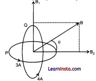
Two identical circular wires P and Q each of radius R and carrying current T are kept in perpendicular planes such that they have a common centre as shown in the figure. Find the magnitude and direction of the net magnetic field at the common centre of the two coils.
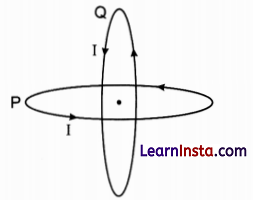
Answer:
Magnetic field produced by the two coils at their common centre having currents I1 and I2 radius a1 and a2, number of turns N1 and N2 respectively are given by :
The resultant field at the common centre is:
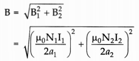
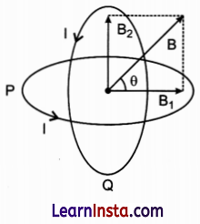
Hence, the net magnetic field is directed at an angle of 45° with either of the fields.
![]()
Question 19.
Calculate the radius of curvature of an equiconcave lens of refractive index 1.5, when it is kept in a medium of refractive index 1.4, to have a power of-5 D?
Answer:
In an equiconcave lens, radius of curvature of both surfaces are equal
∴ \(\frac{1}{f}=(\mu-1)\left(-\frac{1}{R}-\frac{1}{R}\right)\)
Since, P = -5D
Question 20.
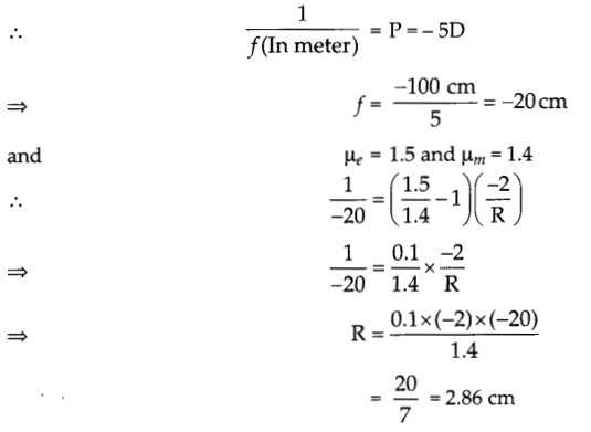
What speed should a galaxy move with respect to us so that the sodium line at 589.0 nm is observed at 589.6 nm ?
Answer:
Therefore, the galaxy is moving away from us.
![]()
Question 21.
In a p-n junction diode the forward bias resistance is low as compared to the reverse bias resistance. Give reason.
OR
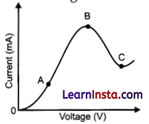
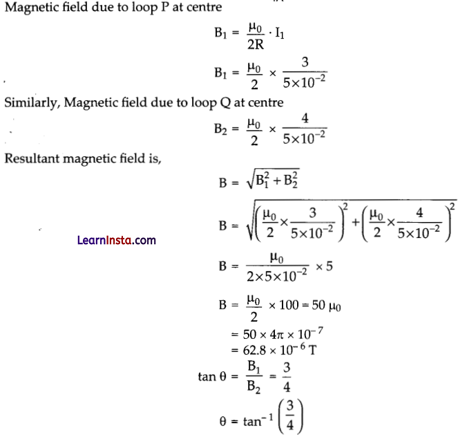
The graph shown in the figure represents a plot of current versus voltage for given semiconductor. Identify the region, if any, over which the semiconductor has a negative resistance.
Answer:
When the p-n junction diode, is forward biased, the diode’s depletion layer or potential barrier shrinks. This can be considered as a practical short circuit.
Hence, resistance is negligible and current flow in forward bias is maximum.
Similarly, when it is reverse bias, depletion layer width (or potential barrier) increases. Hence, resistance increases and very small amount of current flow in reverse bias.
OR
Resistance of a material can be found out by the slope of the V-I curve. Part BC of the curve shows the negative resistance as with the increase in voltage, current decreases.
Section – C
Question 22.
An a.c. source of voltage V = Vo sin ωt is connected to a series combination of L, C and R. Use the phasor diagram to obtain expressions for impedance of the circuit and phase angle between voltage and current. Find the condition when the current will be in phase with the voltage. What is the circuit in this condition called?
OR
In a series LR circuit XL = R and power factor of the circuit is Pi. When capacitor with capacitance C such that XL = Xc is put in series, the power factor becomes P2. Calculate \(\frac{P_1}{P_2}\).
Answer:
Let a series LCR circuit is connected to an a.c. source V (Fig). We take the voltage of the source to be V = Vo sin cof
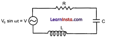
The a.c. current in each element is the same at any time, having the same amplitude and phase. It is given
by,
![]()
Let VL, VR, VC and V represent the voltage across the inductor, resistor, capacitor and the source respectively.
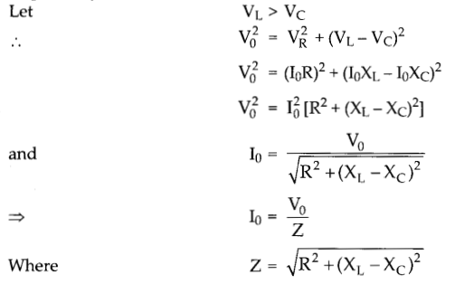
It is called the impedance in an a.c. circuit.
From the figure,
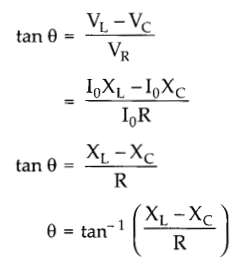
Condition: The current will be in phase with the voltage at resonance condition. At resonance condition,
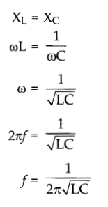
OR
![]()
Question 23.
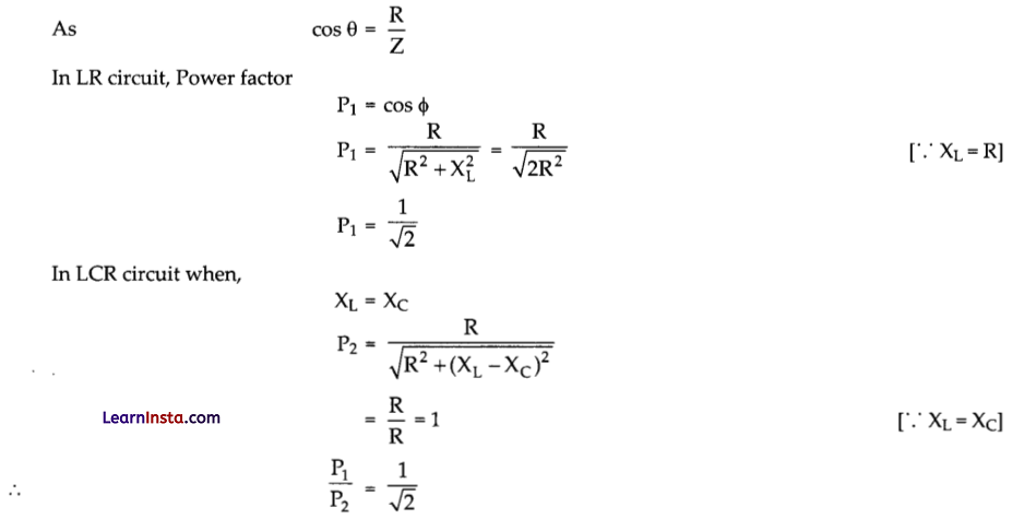
Deduce an expression for the frequency of revolution of a charged particle in a magnetic field and show that it is independent of velocity or energy of the particle.
Answer:
When a charged particle having charge q moves inside a magnetic field \(\overrightarrow{\mathrm{B}}\) having velocity v, it experiences a force, which is given by :
Here, \(\overrightarrow{\mathrm{v}}\) is perpendicular to \(\overrightarrow{\mathrm{B}}\),
F is the force on the charged particle which behaves as the centripetal force and make it move in a circular path.
Let m be the mass of the charged particle and r be the radius of the circular path.
Therefore, the frequency of the revolution of the charged particle is independent of the velocity or the energy of the particle.
Question 24.
Two identical loops P and Q each of radius 5 cm are lying in perpendicular planes such that they have a common centre as shown in the figure. Find the magnitude and direction of the net magnetic field at die common centre of the two coils, if they carry currents equal to 3 A and 4 A respectively.
Answer:
Magnetic field due to loop P at centre
Thus, direction of magnetic field makes an angle 0 with the vertical.
![]()
Question 25.
The given graph shows the variation of photoelectric current (I) versus applied voltage (V) for two different photosensitive materials and for two different intensities of the incident radiations. Identify the pairs of curves that correspond to different materials but same intensity of incident radiation.
OR
Write Einstein photoelectric equation? State clearly the three salient features observe in photoelectric effect, which can be explained on the basis of this equation?
Answer:
Curves 1 and 2 correspond to similar materials while curves 3 and 4 represent different materials, since the value of stopping potential for 1, 2 and 3, 4 are the same. For the given frequency of the incident radiation, the stopping potential is independent of its intensity.
So, the pairs of curves (1 and 3) and (2 and 4) correspond to different materials but same intensity of incident radiation.
OR
Einstein photoelectric equation :
Where \(\phi_0\) is work function. If the energy of the photon absorbed by the electron is less than the work function \(\phi_0\) of the metal, then the electron will not be emitted. Therefore, for the given metal, the threshold frequency of light be vo, then an amount of energy hvo of the photon of light will be spent in ejecting the electron out of the metal, that is, it will be equal to the work function W. Thus,
W= hvo
Thus Ek =hv- hvo
\(\frac{1}{2} m v_{\max }^2=h\left(v-v_0\right)\)
This equation is called ‘Einstein Photoelectric equation’.
Salient features :
(i) The stopping potential and hence the maximum kinetic energy of emitted electrons varies linearly with the frequency of incident radiation.
(ii) There exists a minimum cut-off frequency vo, for which the stopping potential is zero.
(iii) Photoelectric emission is instantaneous.
Question 26.
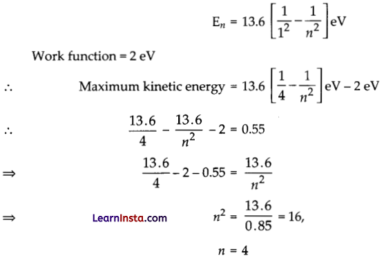
A photon emitted during the de-excitation of electron from a state n the first excited state in a hydrogen atom, irradiates a metallic cathode of work function 2 eV, in a photo cell, with a stopping potential of 0.55 V. Obtain the value of the quantum number of the state n.
Question 27.
Define the distance of closest approach. An a-particle of kinetic energy ‘K’ is bombarded on a thin gold foil. The distance of the closest approach is Y. What will be the distance of closest approach for an a-particle of double the kinetic energy?
Answer:
Distance of closest approach is defined as the minimum distance of the charged particle from the nucleus at which initial kinetic energy of the particle is equal to the potential energy due to the charged nucleus. At this distance,
Kinetic Energy (K) = Potential Energy
![]()
Question 28.
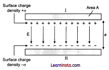
Use Gauss’ law to find the electric field due to a uniformly charged infinite plane sheet. What is the direction of field for positive and negative charge densities?
OR
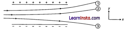
Figure shows tracks of three charged particles in a uniform electrostatic field. Give the signs of the three charges. Which particle has the highest charge to mass ratio?
Answer:
Consider a thin infinite uniformly charged plane sheet having the surface charge density ofa. The electric field is normally outward to the plane sheet and is same in magnitude but opposite in direction.
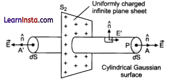
Now, draw a Gaussian surface in the form of cylinder around an axis. Let its cross-sectional area be A. The cylinder is made from three surfaces A, S2, and A’ and the electric flux linked with S2 is 0. So, the total electric flux linked through the Gaussian surface is
\(\phi_E\) = Electric flux through A + Electric flux through S2 + Electric flux through A’
\(\phi_E[/latex = EA cos 0° + 0 + EA cos 0°.
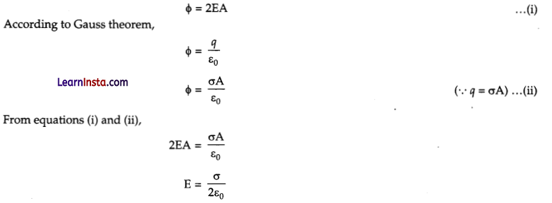
The direction of field for positive charge density is in outward direction and perpendicular to the plane infinite sheet whereas for the negative charge density the direction becomes inward and perpendicular to the sheet.
OR
Opposite charges attract each other and same charges repel each other. It can be observed that particles 1 and 2 both move towards the positively charged plate and repel away from the negatively charged plate. Hence, these two particles are negatively charged. It can also be observed that particle 3 moves towards the negatively charged plate and repels away from the positively charged plate. Hence, particle 3 is positively charged.
The charge to mass ratio (q/m) is directly proportional to the displacement or amount of deflection for a given velocity. Since the deflection of particle 3 is the maximum, it has the highest charge to mass ratio.
Section – D
Question 29.
Sparking Brilliance of Diamond: The total internal reflection of the light is used in polishing diamonds to create a sparking brilliance. By polishing the diamond with specific cuts, it is adjusted the most of the light rays approaching the surface are incident with an angle of incidence more than critical angle. Hence, they suffer multiple reflections and ultimately come out of diamond from the top. This gives the diamond a sparking brilliance.
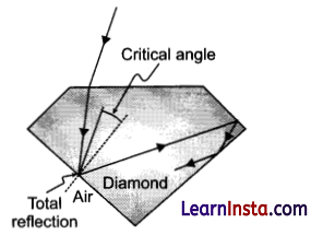
(i) Light cannot easily escape a diamond without multiple internal reflections. This is because:
(a) Its critical angle with reference to air is too large
(b) Its critical angle with reference to air is too small
(c) The diamond is transparent
(d) Rays always enter at angle greater than critical angle
Answer:
(b) Its critical angle with reference to air is too small
(ii) The critical angle for a diamond is 24.4°. Then its refractive index is:
(a) 2.42
(b) 0.413
(c) 1
(d) 1.413
Answer:
(a) 2.42
(iii) The basic reason for the extraordinary sparkle of suitably cut diamond is that:
(a) Low refractive index
(b) High refractive index
(c) High transparency
(d) Very hard
Answer:
(b) High refractive index
(iv) A diamond is immersed in a liquid with a refractive index greater than water. Then the critical angle for total internal reflection will :
(a) Will depend on the nature of the liquid
(b) Remain the same
(c) Decrease
(d) Increases
Answer:
(d) Increases
OR
The following diagram shows same diamond cut in two different shapes.
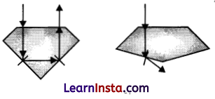
The brilliance of diamond in the second diamond will be:
(a) Less than the first
(b) Greater than first
(c) Same as first
(d) Will depend on the intensity of light
Answer:
(a) Less than the first
![]()
Question 30.
On the basis of energy bands materials are also defined as metals, semiconductor and insulators. In case of metals, conduction band and valence band overlaps with each other due to which electrons are easily available for conduction. In case of insulators, there is some energy gap between conduction band and Valence band due to which no free electrons are easily available for conduction. And in semiconductors, there is a small energy gap between conduction band and Valence band and if we give some external energy then electron from Valence band goes to conduction band due to which conduction will be possible. These semiconductors are classified as intrinsic semiconductors and extrinsic semiconductors and extrinsic semiconductors also. Intrinsic semiconductors are those semiconductors which exist in pure form. And intrinsic semiconductors has number of free electron is equal to number of holes. The semiconductors dopes with some impurity in order to increase its conductivity are called as extrinsic semiconductors doped with pentavalent impurity like Arsenic, Antimony, Phosphorus etc. are called as n-type semiconductors. In n-type semicondoctors electrons are the majority charge carriers and holes are the minority charge carriers.
When trivalent impurity is like Indium, Boron, Aluminium etc. are added to extrinsic semiconductors then p-type semiconductors will be formed. In p-type semiconductors holes are majority charge carriers and electrons are the minority charge carriers.
(i) In case of p-type semiconductors __________
(a) nh«ne
(b) nh=ne
(c) nh» ne
(d) nh=ne = 0
Answer:
(c) rih»ne
(ii) An intrinsic semiconductior behaves like ________ at T = OK.
(a) conductor
(b) metal
(c) non metal
(d) insulator
Answer:
(d) insulator
(iii) If the energy band gap Eg > 3 eV then such materials are called as:
(a) conductors
(b) semiconductors
(c) insulators
(d) superconductors
Answer:
(c) insulators
OR
What is energy band gap in case of materials?
(a) 1.6 ev
(b) 5 ev
(c) zero
(d) 3 ev
Answer:
(c) zero
![]()
(iv) How p-type is formed?
(a) intrinsic semiconductor doped with boron
(b) intrinsic semiconductor doped with aluminium
(c) intrinsic semiconductor doped with antimony
(d) (a) and (b) both
Answer:
(d) (a) and (b) both
(iv) How p-type is formed?
(a) intrinsic semiconductor doped with boron
(b) intrinsic semiconductor doped with aluminium
(c) intrinsic semiconductor doped with antimony
(d) (a) and (b) both
Answer:
(d) (a) and (b) both
Section – E
Question 31.
(a) If one of the two electrons of a H2 molecule is removed, we get a hydrogen molecular ion H2+. In the ground state of an H2+, the two protons are separated by roughly 1.5 A, and the electron is roughly 1 A from each proton. Determine the potential energy of the system. Specify your choice of the zero of potential energy.
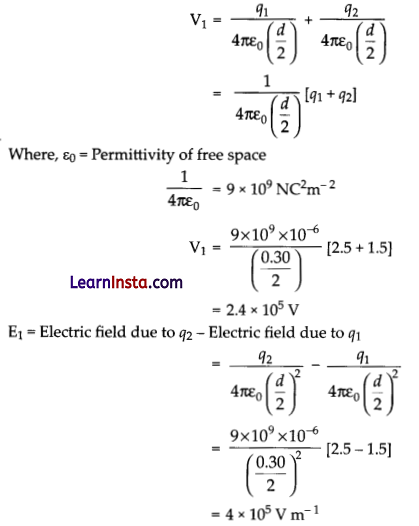
(b) Two tiny spheres carrying charges 1.5 μC and 2.5 μC are located 30 cm apart. Find the potential and electric field:
(i) at the mid-point of the line joining the two charges, and
(ii) at a point 10 cm from this mid-point in a plane normal to the line and passing through the mid point.
OR
(a) (i) Three point charges q,- 4q and 2q are placed at the vertices of an equilateral triangle ABC of side T as shown in the figure. Obtain the expression for the magnitude of the resultant electric force acting on the charge q.
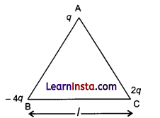
(ii) Find out the amount of the work done to separate the charges at infinite distance.
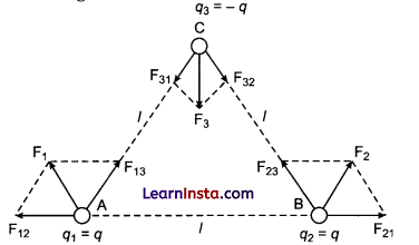
(b) Consider the charges q, q and- q placed at the vertices of an equilateral triangle, as shown in given figure. What is the force on each charge?
Answer:
(a) The system of two protons and one electron is represented in the given figure. The potential energy of the system is,
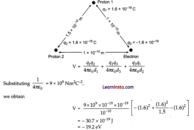
“Therefore, twe potential energy Urine system is -19.2 eV.
![]()
(b) Two charges placed at points A and B are shown in the given figure. O is the mid-point of the line joining the two charges.
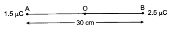
Magnitude of charge located at A,
q1 = 1.5 μC
Magnitude of charge located at B,
q2 = 2.5 μC
Distance between the two charges,
d = 30 cm= 0.3 m
(i) Let V1 and E1 are the electric potential and electric field respectively at O.
V1 = Potential due to charge at A + Potential due to charge at B
Therefore, the potential at mid-point is 2.4 × 10⁵ V and the electric field at mid-point is 4 × 10⁵ Vm-1 The field is directed from the larger charge to the smaller charge.
(ii) Consider a point Z such that normal distance OZ = 10 cm = 0.1 m, as shown in the following figure:
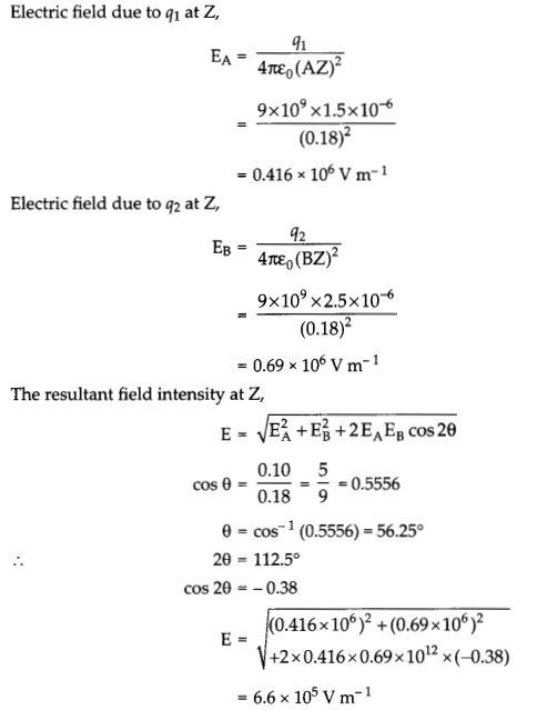
Therefore, the potential at a point 10 cm (perpendicular to the mid-point) is 2.0 × 10⁵ V and electric field is 6.6 × 10⁵ V m-1.
OR
(a) (i) Electric force at A due to charge 2q,
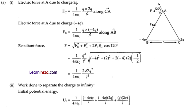
![]()
(ii) Work done to separate the charge to infinity :
Initial potential energy,
(b) The forces acting on charge q at A, due to charges q at B and -q at C are F12 along BA and F13 along AC respectively, as shown in figure from the parallelogram law, the total force F1 on the charge q at A is given by [latex]\mathrm{F}_1=\mathrm{F} \hat{r}_1\) where \(\hat{r}_1\) is a unit vector along BC.
The force of attraction or repulsion for each pair of charges has the same magnitude
The total force F2 on charge q at B is thus \(\mathrm{F}_2=\mathrm{F} \hat{r}_2\) where \(\hat{r}_2\), where is a unit vector along AC.
Similarly, the total force on charge- q at C is F3 = \(\mathrm{F}_3=\sqrt{3} \mathrm{~F} \hat{n}\), where \(\hat{n}\) is the unit vector along the direction bisecting the ZBCA.
It is interesting to see that the sum of the forces on the three charges is zero, i.e.,
F1 + F2 + F3 = 0
Question 32.
(a) Define an equipotential surface. Draw equipotential surfaces:
(i) in the case of a single point charge and,
(ii) in a constant electric field in Z-direction.
Why the equipotential surfaces about a single charge are not equidistant?
(iii) Can electric field exist tangential to an equipotential surface? Give reason.
(b) Show that energy stored in a capacitor is given by E = \(\frac{1}{2} \mathrm{CV}^2\).
OR
(a) If two similar large plates each of area A having surface charge densities + σ and- σ are separated by a distance in air. Find the expressions for:
(i) field at points between the two plates and on outer sides of plates’. Specify the direction of field in each case.
(ii) the potential difference between the plates.
(iii) the capacitance of capacitor so formed.
(b) Figure shows two identical capacitors, C1 and C2 each of 1 μF capacitance connected to a battery of 6 V.
Initially switch ‘S’ is closed. After sometime ‘S’ is left open and dielectric slabs of dielectric constant k = 3 are inserted to fill completely the space between the plates of the two capacitors.
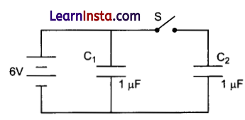
How will the (i) charge and (ii) potential difference between the plates of the capacitors be affected after the slabs are inserted.
Answer:
(a) An equipotential surface is the surface which has same potential at its every point.
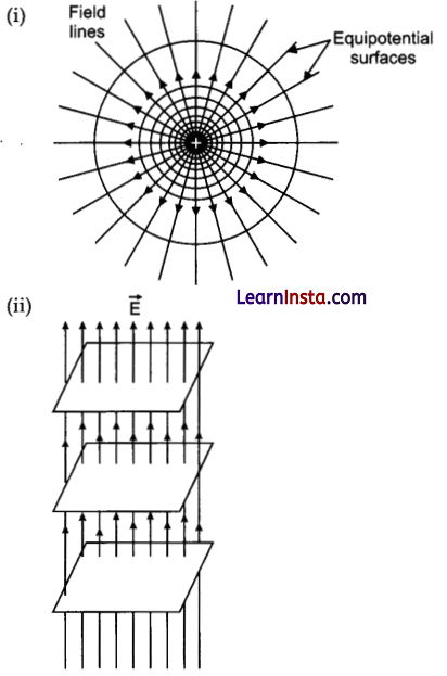
The electric field due to single charge is not constant, this is the reason why the equipotential surfaces about a single charge are not equidistant.
(iii) No, electric field cannot exist tangential to an equipotential surface. If it happen then a charged particle will experience a force along the tangential line and can move along it. As a charged particle can move only due to the potential difference i.e., along the direction of charge of potential, this contradicts the concept of an equipotential surface.
![]()
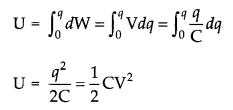
(b) Let the capacitor (C) is connected across a battery of voltage V (volts). The process of charging capacitor is equivalent to transferring charges from one plate to another plate of capacitor.
As soon as charging of capacitor starts there is a potential difference between plates. So to transfer charges against the potential difference some work is to be done and this work gets stored as electrostatic potential energy in capacitor.
Let dq be the charge transferred against the potential difference V, then work done is
dW=Vdq
\(=\frac{q}{C} d q\)Total work done to transfer charge q, is
OR
(a) (i) Consider a parallel plate capacitor with two identical plates X and Y, each having an area of A, and separated by a distance d. Let the space between the plates be filled by a dielectric medium with its dielectric constant as K and a be the surface charge density on each of the plates.
Surface charge density of plate 1
\(\sigma=\frac{Q}{A}\)
and that of plate 2 is σ.
Electric field in outer region I,
Electric field in outer region II,
\(\mathrm{E}=\frac{\sigma}{2 \varepsilon_0}-\frac{\sigma}{2 \varepsilon_0}=0\)The inner region between plates 1 and 2. In the electric fields due to the two charged plates add up.
So,
\(\mathrm{E}=\frac{\sigma}{2 \varepsilon_0}+\frac{\sigma}{2 \varepsilon_0}=\frac{\sigma}{\varepsilon_0}\)
(ii) For uniform electric field potential difference is simply the electric field multiplied by the distance between the plates, i.e.,
\(\mathrm{V}=\mathrm{E} d=\frac{1}{\varepsilon_0} \frac{\mathrm{Q} d}{\mathrm{~A}}\)
(iii) Capacitance of parallel plates capacitor,
(b) When, switch ‘S’ is closed,
Potential difference across C1 = Potential difference across C2 = 6 V
V1 = V2 = 6V
q1 = q2 = 1 μF × 6V = 6 μC
When switch ‘S’ is opened, the potential difference across Q remains 6 V, while the charge on capacitor C2 remains 6 μC.
After insertion of dielectric slab (k = 3) between the plates of each capacitor, the new capacitance of each capacitor becomes
C’1 = 3 × 1 μF = 3 μF
C’2 = 3 μF
(i) Now, charge on capacitor Q,
q’1 = C’1V1 = 3 × 6 = 18 μC
![]()
(ii) When S is open, potential difference across C2
\(\mathrm{V}_2^{\prime}=\frac{q_2}{\mathrm{C}_2^{\prime}}=\frac{6 \mu \mathrm{C}}{3 \mu \mathrm{F}}=2 \mathrm{~V}\)Question 33.
(a) Draw the ray diagram showing refraction of ray of light through a glass prism. Derive the expression for the refractive index μ of the material of prism in terms of the angle of prism A and angle of minimum deviation δm.
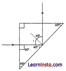
(b) A ray of light PQ enters an isosceles right-angled prism ABC of refractive index 1.5 as shown in figure.
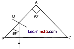
(i) Trace the path of the ray through the prism.
(ii) What will be the effect on the path of the ray if the refractive index of the prism is 1.4?
OR
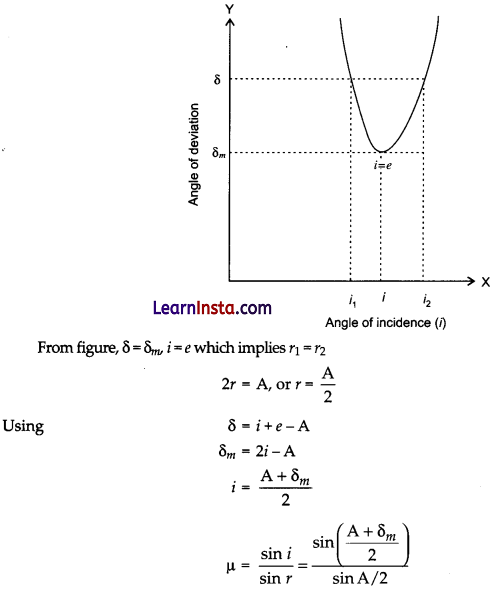
(a) Plot a graph to show variation of the angle of deviation as a function of angle of incidence for light passing through a prism. Derive an expression for refractive index of the prism in terms of angle of minimum deviation and angle of prism.
(b) (i) What is dispersion of light? What is its cause?
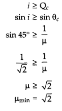
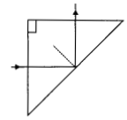
(ii) A ray of light incident normally on one face of a right isosceles prism is totally reflected as shown in fig. What must be the minimum value of refractive index of glass ? Give relevant calculations.
Answer:
PQ = incident ray
QR = refracted ray
RS = emergent ray
∠A = angle of prism
∠ i = angle of incidence
∠r1 = angle of refraction
∠e = angle of emergence
∠δ = angle of deviation
Consider, the above diagram and p as the refractive index of the prism.
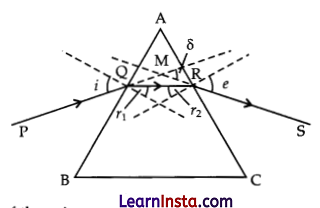
In case of minimum deviation, ∠r1 = ∠r2 = ∠r
and A = ∠r1 + ∠r2
So, A = ∠r+ ∠r = 2∠r
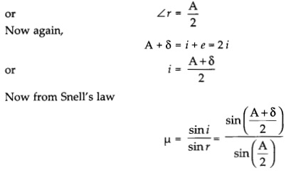
is the required expression.
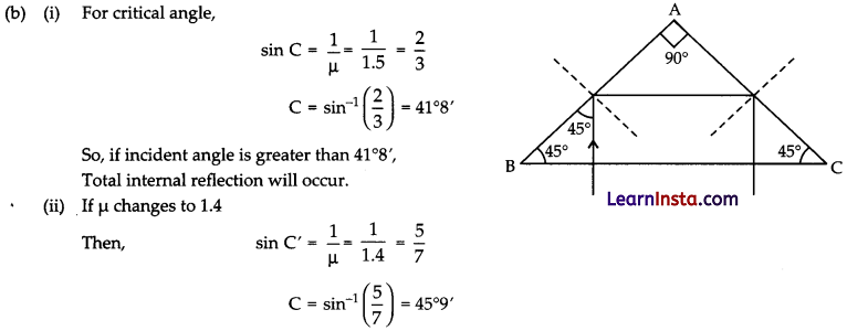
Since, incident angle is less than the critical angle. Then total internal reflection will not occur.
OR
(a)
![]()
(b) (i) Dispersion of Light: Dispersion is often observed as light passes through a triangular prism. Upon passing through the prism, the white light is separated into its component colours, red, orange, yellow, green, blue, indigo and violet. The separation of visible light into its different colours is known as dispersion. Dispersion occurs because for different colour of light, a transparent medium will have different refractive indices (μ) as different colours have different speed of light in transparent medium.
(ii) For total internal reflection: